Smartkem Collaborates with Manz Asia for Advanced Computer and AI Chip Packaging Solutions

Manz Asia will be demonstrating its advanced inkjet metallization using Smartkem's advanced dielectric materials at SEMICON® SEA 2025 in Singapore, May 20-22, 2025.
Visit Manz Asia at Booth no. L1314.
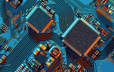
MANCHESTER, England, May 19, 2025 /PRNewswire/ -- Smartkem (Nasdaq: SMTK), which is seeking to change the world of electronics with a new class of transistor technology, today announced that it has entered into a collaboration with Manz Asia, a developer of production solutions for semiconductor advanced packaging manufacturing sectors. The collaboration includes the demonstration of inkjet printable dielectric layers for use in advanced computer and AI chip packaging solutions at this year's SEMICON® SEA in Singapore, May 20-22, 2025.
Smartkem Chairman and CEO, Ian Jenks, commented: "We're thrilled to be working with Manz Asia to address a fast-growing opportunity in the market for advanced computer and AI chip packaging. As the demand for AI leads to increasingly complex servers, our materials combined with Manz Asia's printing technology have the potential to enable large area panel chip packaging beyond the existing constraints of today's 300mm wafer packaging. Panel level packaging is a market expected to grow to approximately $600 million in 2030, a 27% compound annual growth rate from 2024. "[1]
Manz Asia General Manger, Robert Lin, commented: "Manz Asia is committed to advancing green manufacturing and smart production through the development of high-precision inkjet printing equipment. Our maskless inkjet technology enables accurate material deposition and supports a wide range of inks, making it suitable for various substrates—including PI, ABF, EMC, silicon, and glass—in both wafer and panel formats. The collaboration with Smartkem marks a significant step in demonstrating how our inkjet platform, combined with next-generation dielectric materials, can deliver scalable and sustainable solutions for semiconductor advanced packaging."
Building on the UV curable dielectric layer chemistry developed at Smartkem's R&D facility for thin film transistor fabrication, Smartkem has designed ink formulations suitable for use in advanced computer and AI chip packaging applications. These inks have been co-developed with Manz Asia to be compatible with its existing inkjet-based semiconductor production equipment.
Panel level packaging on rectangular wafers offers key advantages over traditional packaging on circular wafers, including:
- Higher throughput, as a larger print area means more chips can be packaged simultaneously;
- Lower cost per chip from economies of scale with use of printed circuit board like manufacturing equipment;
- Better material utilization from less edge loss compared to circular wafers; and
- Improved integration supported by complex fan-out wafer-level packaging at a larger scale.
About Smartkem
Smartkem is seeking to change the world of electronics with a new class of transistors developed using its proprietary advanced semiconductor materials. Our TRUFLEX® semiconductor polymers enable low temperature printing processes that are compatible with existing manufacturing infrastructure to deliver low-cost, high-performance displays. Our semiconductor platform can be used in a range of display technologies including MicroLED, LCD and AMOLED, as well as in applications in advanced computer and AI chip packaging, sensors, and logic.
Smartkem designs and develops its materials at its research and development facility in Manchester, UK and provides prototyping services at the Centre for Process Innovation (CPI) in Sedgefield, UK. It operates a field application office in Hsinchu, Taiwan, close to collaboration partner, The Industrial Technology Research Institute (ITRI). Smartkem is developing a commercial-scale production process and Electronic Design Automation (EDA) tools to demonstrate the commercial viability of manufacturing a new generation of displays using its materials.
The company has an extensive IP portfolio including 138 granted patents across 17 patent families, 16 pending patents and 40 codified trade secrets. For more information, visit our website or follow us on LinkedIn.
About Manz Asia
Manz Asia is a leading manufacturer of advanced semiconductor equipment, driving technological innovation and process excellence within the CoPoS (CoWoS panelization) technology framework for panel-level packaging.
We offer comprehensive equipment solutions encompassing wet chemistry, plating, digital printing, automation, and proprietary software integration for Redistribution Layer (RDL) process—from lab-scale to mass production. Our technologies support key applications in Fan-Out Panel-Level Packaging (FOPLP), Through Glass Via (TGV), and IC substrates, covering critical stages of semiconductor packaging.
By enhancing production efficiency, optimizing process quality, and strengthening market competitiveness, Manz Asia empowers the semiconductor industry to achieve higher standards of excellence.
For more information, please visit website or follow us on LinkedIn.
About SEMICON® Southeast Asia
Forward-thinking semiconductor organizations are implementing practices to reduce the environmental impact of their businesses and manufacturing operations to ensure their resiliency when disruptive events such as geopolitical conflicts, climate-related disasters, and public health crises strike. Initiatives focused on reducing greenhouse gas emissions and water use, deploying renewable energy systems, and improving the energy efficiency of chipmaking equipment are growing in importance.
To thrive in the coming decade and beyond, companies must look beyond short-term performance and focus on building resilience to better withstand unpredictable disruptions to their businesses, the semiconductor industry and global economies. Visit the website for more information.
Forward-Looking Statements
All statements in this press release that are not historical are forward-looking statements, including, among other things, its market position and market opportunity, expectations and plans as to its product development, manufacturing and sales, and relations with its partners and investors. These statements are not historical facts but rather are based on Smartkem, Inc.'s current expectations, estimates, and projections regarding its business, operations and other similar or related factors. Words such as "may," "will," "could," "would," "should," "anticipate," "predict," "potential," "continue," "expect," "intend," "plan," "project," "believe," "estimate," and other similar or elated expressions are used to identify these forward-looking statements, although not all forward-looking statements contain these words. You should not place undue reliance on forward-looking statements because they involve known and unknown risks, uncertainties, and assumptions that are difficult or impossible to predict and, in some cases, beyond the Company's control. Actual results may differ materially from those in the forward-looking statements as a result of a number of factors, including those described in the Company's filings with the Securities and Exchange Commission. The Company undertakes no obligation to revise or update information in this release to reflect events or circumstances in the future, even if new information becomes available.
Industry Representatives and Media
Selena Kirkwood
Head of Communications for Smartkem
T: +44 (0) 7971 460 364
s.kirkwood@smartkem.com
Analysts and Investors
David Barnard, CFA
Alliance Advisors Investor Relations
T: 1 415 433 3777
dbarnard@allianceadvisors.com
[1] Yole Intelligence: Panel Level Packaging 2025 https://www.yolegroup.com/product/report/panel-level-packaging-2025/
Logo - https://mma.prnewswire.com/media/2597198/5324096/SmartKem_Brand_Identity_RGB_POS___small_Logo.jpg


Share this article