From Concept to Mass Production: Risen Energy's Journey with Ultra-Thin Wafers

NINGBO, China, March 11, 2026 /PRNewswire/ -- As discussions about "space photovoltaics" continue to ripple across the industry, several key technical attributes are repeatedly emphasized: lightweight design, high-power output, radiation resistance, and long-term reliability. These requirements naturally direct our focus to a core technology we have long been developing and have already deployed at scale—the application of ultra-thin silicon wafers in Heterojunction (HJT) solar cells.
Today, as we revisit the technical white paper released by Risen Energy— Risen Energy's HJT Hyper-ion: A White Paper on Development and Industrial Application of Ultra-Thin Silicon Wafers —we find that many of the ideas now emerging in frontier were already embedded in the practical engineering logic documented there. This comprehensive record from the mass production front may offer the industry a perspective that combines technical insights and practical support.
1. Why "Thin"? An Inevitable Choice Rooted in Structural Nature
In the white paper, we clearly point out that in the cost structure of HJT solar cells, silicon wafers account for the largest proportion at 55%. Therefore, wafer thinning is the most direct and effective method for cost reduction. However, the rationale goes beyond economics. It is fundamentally tied to the nature of HJT technology itself.
HJT's entire low-temperature manufacturing process (<200°C) and its fully symmetrical cell structure allow the wafer to be processed in a much "gentler" manner, which significantly reduce risks such as wafer warping and breakage issues caused by high-temperature processes and asymmetric stress inherent in PERC and TOPCon technologies. In this sense, ultra-thin wafers are not merely compatible with HJT — they are an inherent advantage of HJT technology, and one of the key enablers for its broader future applications.
2. How can "Thin" Remain Reliable? Systematic Balance of Efficiency, Yield, and Mechanical Strength
We have conducted a series of explorations and practices focusing on efficiency, production yield rate, and mechanical strength:
2.1 Efficiency Trade-offs
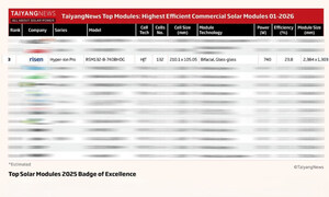
Our experiments results, consistent with findings in industry literature, reveal an interesting "seesaw" relationship: while short-circuit current (Jsc) decreases with wafer thinning, open-circuit voltage (Voc) increases. The fill factor (FF) remains relatively constant. Within a specific "plateau" phase, the overall cell efficiency decline is minimal and acceptable. The width of this plateau varies across different cell technologies. For Risen Energy, HJT Hyper-ion cells manufactured with 110 μm wafers have already achieved an average efficiency of 26.4%, with the best production batches exceeding 26.6%. These results demonstrate that, for HJT technology, proper wafer thinning does not compromise the upper limit of performance.
2.2 Manufacturing Optimization
We redesigned the wafer cassette configuration, switching from horizontal insertion to vertical insertion, while optimizing all related automation and transfer processes across the line. The results show a stabilized yield rate consistently above 99.5% with a fragment rate below 0.25%, proving that manufacturing challenges posed by "wafer thinning" can be overcome through systematic process and equipment innovation.
2.3 Mechanical Strength Rediscovery
Our comparative tests revealed that 150μm PERC and 130μm TOPCon cells fractured during bending test. However, when the thickness was reduced to below 100 μm, the cells instead exhibited excellent flexibility. HJT cells exhibit exceptional flexibility, creating new possibilities for lightweight modules and special environment applications.
3. From Ground to Space: Extending the Depth of "Thin"
Our current mass-produced HJT Hyper-ion products for ground-mounted power plants fully utilize 110μm silicon wafers, and solar cell thickness of approximately 95μm. At this thickness level, we have achieved optimal balance in efficiency, yield and reliability with significant cost reduction. Yet this represents only one aspect of our technical capability.
Notably, for space photovoltaic applications, where an extremely high power-to-weight ratios is required, solar cells typically need to be 70μm or even thinner. Thanks to years of accumulated expertise in HJT ultra-thin wafer technology, Risen Energy has developed the capability to produce cells below 70μm.
4. Making "Thin" Work Effectively? System Innovation from Cell to Module
Conventional high-temperature soldering is no longer suitable for such thin cells. To address this challenge, Risen Energy pioneered the Hyper-link stress-free cell interconnection technology. Protected by over 50+ exclusive patents, this technology avoids soldering thermal stress, perfectly matching HJT's low-temperature characteristics and ultra-thin cells' physical properties.
This innovation is backed by rigorous reliability testing, far exceeding IEC standards: 5400Pa static load, 10,000 dynamic load cycles, 2000 hours of damp heat (DH2000), 400 thermal cycles (TC400), and other accelerated aging tests. Results confirmed that Hyper-ion modules using ultra-thin wafers and Hyper-link technology show power degradation performance degradation far below standard requirements.
5. Integrated R&D
Reflecting on this journey toward ultra-thin wafers, the core lies not only in individual technological breakthroughs but also in integrated innovation across wafers, cells, and modules. Wafer thinning, low-silver metallization, zero-busbar cells, and Hyper-link technologies interconnect like puzzle pieces under unified design, ultimately forming Hyper-ion products' complete competitiveness.
Risen Energy's ultra-thin wafer journey began responding to industrial cost-reduction needs and succeeded through respect for technological essence and commitment to systematic innovation. By revisiting and sharing this white paper, we hope to present our current stage of reflection and industrial practice, and to work together with partners across the industry to drive photovoltaic technology toward a future that is lighter, stronger, and more imaginative than ever before.


Share this article